Small-signal AC analysis of a silicon PIN photodiode#
Introduction to Small-signal Analysis#
Small-Signal AC (SSAC) analysis is a technique used to characterize the frequency-dependent behavior of semiconductor devices under small perturbations around a DC operating point. This method is essential for understanding the high-frequency performance limitations of devices such as photodiodes, modulators, and transistors. We first establish a DC operating point (bias condition) for the device. Then, we apply a small AC voltage perturbation and analyze how the device responds at different frequencies. The analysis assumes that the perturbation is small enough that the device’s response remains linear, allowing us to extract frequency-dependent parameters.
The primary output of SSAC analysis is the small-signal admittance $ Y(\omega) $, which relates the small-signal current $ I(\omega) $ to the small-signal voltage $ V(\omega) $:
where:
$ G(\omega) $ is the conductance (real part of admittance), representing resistive losses
$ C(\omega) $ is the capacitance (imaginary part divided by \(\omega\)), representing charge storage
$ \omega `= 2:nbsphinx-math:pi `f $ is the angular frequency
Goal of this notebook#
In this notebook, we will:
Set up a reverse-biased silicon PIN photodiode structure
Perform SSAC analysis over a range of frequencies
Extract and plot the frequency-dependent conductance $ G(f) $ and capacitance $ C(f) $
Setup and imports#
[1]:
import matplotlib.pyplot as plt
import numpy as np
import tidy3d as td
import tidy3d.web as web
Device and simulation setup#
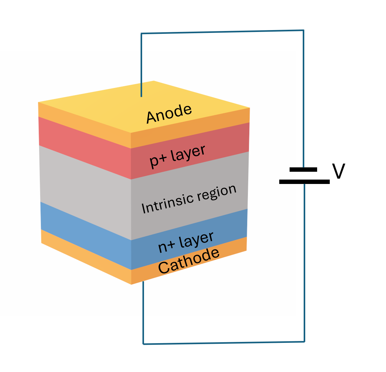
PIN photodiode structure#
We will design a vertical PIN photodiode with the following structure:
P+ region: Heavily doped p-type silicon (top contact)
Intrinsic region: Lightly doped silicon (absorption region)
N+ region: Heavily doped n-type silicon (bottom contact)
Metal contacts: Aluminum electrodes for electrical connection
The device will be operated under reverse bias (negative voltage on p-side), which depletes the intrinsic region and creates a strong electric field for efficient photocarrier collection.
Geometry definition#
First, we define the geometric parameters of our PIN structure. All dimensions are in micrometers (µm).
[2]:
# Device dimensions (µm)
device_width = 2.0  # Lateral dimension
z_size = 2.0  # Extrusion dimension (for 2D simulation)

# Layer thicknesses
p_thickness = 0.3  # P+ contact layer
i_thickness = 1.0  # Intrinsic absorption region
n_thickness = 0.3  # N+ contact layer
contact_thickness = 0.2  # Metal contact thickness

# Layer centers (stacked vertically along y-axis)
total_height = p_thickness + i_thickness + n_thickness
y_bottom = -total_height / 2

# N+ layer (bottom)
n_center_y = y_bottom + n_thickness / 2
n_center = (0, n_center_y, 0)
n_size = (device_width, n_thickness, z_size)

# Intrinsic layer (middle)
i_center_y = n_center_y + n_thickness / 2 + i_thickness / 2
i_center = (0, i_center_y, 0)
i_size = (device_width, i_thickness, z_size)

# P+ layer (top)
p_center_y = i_center_y + i_thickness / 2 + p_thickness / 2
p_center = (0, p_center_y, 0)
p_size = (device_width, p_thickness, z_size)

# Contact layers
contact_n_y = n_center_y - n_thickness / 2 - contact_thickness / 2
contact_p_y = p_center_y + p_thickness / 2 + contact_thickness / 2

contact_n_center = (0, contact_n_y, 0)
contact_p_center = (0, contact_p_y, 0)
contact_size = (device_width, contact_thickness, z_size)
Doping profile#
Next, we define the doping profiles for the PIN structure. We use:
Constant doping for the lightly doped intrinsic region (background doping)
Gaussian doping for the heavily doped P+ and N+ regions with smooth transitions
The doping concentrations are based on typical values for silicon photodiodes.
[3]:
# Doping concentrations (cm^-3)
intrinsic_doping = 1e14  # Background doping in intrinsic region
p_plus_doping = 1e19  # P+ contact doping
n_plus_doping = 1e19  # N+ contact doping

# Junction width for Gaussian doping profiles
junction_width = 0.01  # Controls sharpness of doping transition

# Intrinsic region: constant low doping
acceptor_intrinsic = td.ConstantDoping(center=i_center, size=i_size, concentration=intrinsic_doping)

# P+ region: Gaussian acceptor doping
acceptor_p_plus = td.GaussianDoping(
    center=p_center,
    size=p_size,
    concentration=p_plus_doping,
    ref_con=intrinsic_doping,
    width=junction_width,
    source="ymax",  # Doping is constant along ymax plane
)

# N+ region: Gaussian donor doping
donor_n_plus = td.GaussianDoping(
    center=n_center,
    size=n_size,
    concentration=n_plus_doping,
    ref_con=intrinsic_doping,
    width=junction_width,
    source="ymin",  # Doping is constant along ymin plane
)
Material models#
We now define the physical models for silicon. The parameters are based on well-established models from semiconductor device physics literature.
[4]:
# Electron mobility model (Caughey-Thomas)
mobility_n = td.CaugheyThomasMobility(
    mu=1471.0,  # Maximum mobility (cm²/V·s)
    mu_min=52.2,  # Minimum mobility (cm²/V·s)
    ref_N=9.68e16,  # Reference doping (cm⁻³)
    exp_N=0.68,  # Doping exponent
    exp_1=-0.57,  # Temperature exponent 1
    exp_2=-2.33,  # Temperature exponent 2
    exp_3=2.4,  # Temperature exponent 3
    exp_4=-0.146,  # Temperature exponent 4
)

# Hole mobility model (Caughey-Thomas)
mobility_p = td.CaugheyThomasMobility(
    mu=470.5,  # Maximum mobility (cm²/V·s)
    mu_min=44.9,  # Minimum mobility (cm²/V·s)
    ref_N=2.23e17,  # Reference doping (cm⁻³)
    exp_N=0.719,  # Doping exponent
    exp_1=-0.57,  # Temperature exponent 1
    exp_2=-2.23,  # Temperature exponent 2
    exp_3=2.4,  # Temperature exponent 3
    exp_4=-0.146,  # Temperature exponent 4
)

# Effective density of states (constant for isothermal simulation)
# Values at T=300K from Sze & Ng
N_c = td.ConstantEffectiveDOS(N=2.86e19)  # Conduction band (cm⁻³)
N_v = td.ConstantEffectiveDOS(N=3.1e19)  # Valence band (cm⁻³)

# Energy bandgap at 300K
E_g = td.ConstantEnergyBandGap(eg=1.12)  # Silicon bandgap (eV)
Recombination models#
We include the major recombination mechanisms in silicon:
Shockley-Read-Hall (SRH): Recombination through trap states.
Radiative: Band-to-band recombination.
Auger: Three-particle recombination.
[5]:
# Shockley-Read-Hall recombination
# Carrier lifetimes for moderately pure silicon
srh_recombination = td.ShockleyReedHallRecombination(
    tau_n=1e-6,  # Electron lifetime (s)
    tau_p=1e-6,  # Hole lifetime (s)
)

# Radiative recombination
radiative_recombination = td.RadiativeRecombination(
    r_const=1.6e-14  # Radiative recombination coefficient (cm³/s)
)

# Auger recombination
auger_recombination = td.AugerRecombination(
    c_n=2.8e-31,  # Electron Auger coefficient (cm⁶/s)
    c_p=9.9e-32,  # Hole Auger coefficient (cm⁶/s)
)
Bandgap Narrowing#
Since we have high doping levels in the contact regions, bandgap narrowing is expected to impact the device characteristics. We take this effect into consideration by applying the Slotboom model.
[6]:
# Bandgap narrowing model (Slotboom)
bandgap_narrowing = td.SlotboomBandGapNarrowing(
    v1=6.92e-3,  # Narrowing coefficient (eV)
    n2=1.3e17,  # Reference concentration (cm⁻³)
    c2=0.5,  # Exponent
    min_N=1e15,  # Minimum doping for narrowing (cm⁻³)
)
Create MultiPhysics Media#
We now assemble all the material properties into MultiPhysicsMedium objects for use in the simulation.
[7]:
# Silicon semiconductor medium with all doping and physical models
si_charge = td.SemiconductorMedium(
    permittivity=11.7,
    N_c=N_c,
    N_v=N_v,
    E_g=E_g,
    N_d=[donor_n_plus],  # List of donor doping profiles
    N_a=[acceptor_intrinsic, acceptor_p_plus],  # List of acceptor doping profiles
    mobility_n=mobility_n,
    mobility_p=mobility_p,
    R=[srh_recombination, radiative_recombination, auger_recombination],
    delta_E_g=bandgap_narrowing,
)

# Silicon as a MultiPhysicsMedium
Si_medium = td.MultiPhysicsMedium(charge=si_charge, name="Si_doped")

# Aluminum contacts (high conductivity metal)
Al_medium = td.MultiPhysicsMedium(
    charge=td.ChargeConductorMedium(conductivity=3.5e7 * 1e-6),  # Convert to µm units
    name="Al",
)

# Air as background medium
air = td.MultiPhysicsMedium(name="air")
Create Geometry Structures#
[8]:
# Silicon structures
si_p_structure = td.Structure(
    geometry=td.Box(center=p_center, size=p_size), medium=Si_medium, name="si_p_region"
)

si_i_structure = td.Structure(
    geometry=td.Box(center=i_center, size=i_size), medium=Si_medium, name="si_i_region"
)

si_n_structure = td.Structure(
    geometry=td.Box(center=n_center, size=n_size), medium=Si_medium, name="si_n_region"
)

# Metal contact structures
contact_p_structure = td.Structure(
    geometry=td.Box(center=contact_p_center, size=contact_size), medium=Al_medium, name="contact_p"
)

contact_n_structure = td.Structure(
    geometry=td.Box(center=contact_n_center, size=contact_size), medium=Al_medium, name="contact_n"
)

# Combine all structures
structures = [
    si_n_structure,
    si_i_structure,
    si_p_structure,
    contact_n_structure,
    contact_p_structure,
]
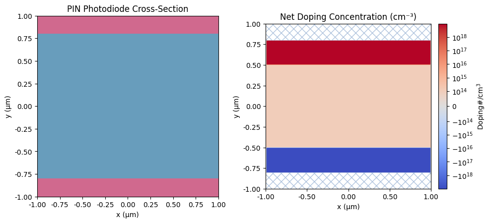
Visualize the Device Structure#
Before running the simulation, let’s visualize the device geometry and doping profile.
[9]:
# Create scene for visualization
scene = td.Scene(structures=structures, medium=air)

# Plot geometry and doping
fig, (ax1, ax2) = plt.subplots(1, 2, figsize=(10, 5))

# Plot structure geometry
scene.plot(z=0, ax=ax1)
ax1.set_title("PIN Photodiode Cross-Section")
ax1.set_xlabel("x (µm)")
ax1.set_ylabel("y (µm)")

# Plot doping profile
scene.plot_structures_property(z=0, property="doping", ax=ax2, scale="symlog")
ax2.set_title("Net Doping Concentration (cm⁻³)")
ax2.set_xlabel("x (µm)")
ax2.set_ylabel("y (µm)")

plt.tight_layout()
plt.show()
Boundary conditions and SSAC analysis setup#
Now we define the electrical boundary conditions for the SSAC analysis:
Cathode (N-contact): Grounded at 0V.
Anode (P-contact): SSAC analysis voltage source with DC bias and small-signal perturbation.
We apply a reverse bias to the photodiode to:
Deplete the intrinsic region.
Create a strong electric field for fast carrier collection.
Minimize junction capacitance.
[10]:
# DC bias voltages for reverse bias operation
reverse_bias_voltages = [-2]  # -2V reverse bias

# Small-signal amplitude (must be small for linear approximation)
ac_amplitude = 1e-3  # 1 mV perturbation

# Cathode: ground reference (N-contact)
bc_cathode = td.HeatChargeBoundarySpec(
    condition=td.VoltageBC(source=td.GroundVoltage()),
    placement=td.StructureStructureInterface(structures=["contact_n", "si_n_region"]),
)

# Anode: SSAC voltage source (P-contact)
bc_anode = td.HeatChargeBoundarySpec(
    condition=td.VoltageBC(
        source=td.SSACVoltageSource(voltage=reverse_bias_voltages, amplitude=ac_amplitude)
    ),
    placement=td.StructureStructureInterface(structures=["contact_p", "si_p_region"]),
)

boundary_specs = [bc_cathode, bc_anode]
Frequency range for SSAC analysis#
We define a logarithmic frequency sweep from 100 Mhz to 100 GHz to capture the frequency-dependent behavior.
[11]:
# Frequency range for SSAC analysis (Hz)
freq_min = 1e8  # 100 Mhz
freq_max = 1e11  # 100 GHz
n_freqs_per_decade = 5  # Number of frequency points per decade

freq_range = td.FreqRange.from_freq_interval(freq_min, freq_max)
freqs = freq_range.sweep_decade(n_freqs_per_decade)
Define Monitors#
We set up monitors to record various quantities during the simulation.
[12]:
# Monitor for free carrier concentration
carrier_monitor = td.SteadyFreeCarrierMonitor(
    center=(0, 0, 0), size=(td.inf, td.inf, td.inf), name="carriers", unstructured=True
)

# Monitor for electric potential
potential_monitor = td.SteadyPotentialMonitor(
    center=(0, 0, 0), size=(td.inf, td.inf, td.inf), name="potential", unstructured=True
)

monitors = [carrier_monitor, potential_monitor]
Analysis and Solver Settings#
We configure the SSAC analysis parameters and solver tolerance settings.
[13]:
# Solver tolerance settings
charge_tolerance = td.ChargeToleranceSpec(
    rel_tol=1e-5,  # Relative tolerance
    abs_tol=1e16,  # Absolute tolerance (cm⁻³)
    max_iters=400,  # Maximum iterations
    ramp_up_iters=1,  # Ramping iterations for convergence
)

# SSAC analysis specification
analysis_spec = td.IsothermalSSACAnalysis(
    tolerance_settings=charge_tolerance,
    convergence_dv=0.1,  # Voltage convergence criterion (V)
    fermi_dirac=False,  # Use Maxwell-Boltzmann statistics (faster, adequate for moderate doping)
    temperature=300,  # Ambient temperature (K)
    freqs=freqs.tolist(),  # Frequency list for AC analysis
)
Grid specification#
We define the mesh for the simulation. A finer mesh near the junctions ensures accurate resolution of the space-charge regions where the electric field varies rapidly.
[14]:
# Base mesh resolution
dl_bulk = 0.04  # Bulk mesh size (µm)
dl_interface = 0.015  # Interface mesh size (µm)

# Refined regions near P-I and I-N junctions
refinement_pi = td.GridRefinementRegion(
    center=(0, p_center_y - p_thickness / 2, 0),
    size=(device_width, 0.2, 0),
    dl_internal=dl_interface / 2,
    transition_thickness=dl_bulk * 10,
)

refinement_in = td.GridRefinementRegion(
    center=(0, n_center_y + n_thickness / 2, 0),
    size=(device_width, 0.2, 0),
    dl_internal=dl_interface / 2,
    transition_thickness=dl_bulk * 10,
)

# Grid specification
grid_spec = td.DistanceUnstructuredGrid(
    relative_min_dl=0,
    dl_interface=dl_interface,
    dl_bulk=dl_bulk * 20,
    distance_interface=2 * dl_interface,
    distance_bulk=6 * dl_interface,
    sampling=1000,
    uniform_grid_mediums=["Si_doped"],
    mesh_refinements=[refinement_pi, refinement_in],
)
Create the Simulation#
Finally, we assemble all components into a HeatChargeSimulation object.
[15]:
# Simulation domain
sim_center = (0, 0, 0)
sim_size = (device_width * 1.2, total_height + 2 * contact_thickness + 0.2, 0)

# Create simulation
sim = td.HeatChargeSimulation(
    medium=air,
    structures=structures,
    size=sim_size,
    center=sim_center,
    boundary_spec=boundary_specs,
    analysis_spec=analysis_spec,
    monitors=monitors,
    grid_spec=grid_spec,
)
Run the Simulation#
Now we run the SSAC simulation using the Tidy3D backend solver. The simulation will first solve the DC problem at the specified bias voltage. Then, it will perform small-signal analysis at each frequency and extract AC current response.
[16]:
results = web.run(sim)
11:57:29 CET Created task 'heat_charge_2025-12-09_11-57-28' with resource_id
             'hec-f88de0e2-0f8a-465b-bd90-b94d7118d156' and task_type
             'HEAT_CHARGE'.
             Tidy3D's HeatCharge solver is currently in the beta stage. Cost of
             HeatCharge simulations is subject to change in the future.
11:57:39 CET Estimated FlexCredit cost: 0.025. Minimum cost depends on task
             execution details. Use 'web.real_cost(task_id)' to get the billed
             FlexCredit cost after a simulation run.
11:57:42 CET status = queued
             To cancel the simulation, use 'web.abort(task_id)' or
             'web.delete(task_id)' or abort/delete the task in the web UI.
             Terminating the Python script will not stop the job running on the
             cloud.
11:58:05 CET status = preprocess
11:59:00 CET starting up solver
running solver
12:06:04 CET status = success
12:06:08 CET Loading simulation from simulation_data.hdf5
Post-processing and results analysis#
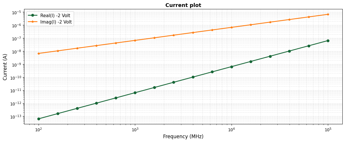
Extract AC current data#
The SSAC simulation provides complex-valued AC current \(I(v, f)\) as a function of DC bias voltage \(v\) and frequency \(f\) . This current represents the device’s small-signal response to the AC voltage perturbation.
[17]:
# Extract AC current-voltage data
ac_current = -results.device_characteristics.ac_current_voltage

# Get the bias voltage and frequency arrays
bias_voltage = reverse_bias_voltages[0]

frequencies = ac_current.coords["f"].values  # Frequency array

# Select current at the specified bias voltage
# Note: For 2D simulations, multiply by device depth to get total current
device_depth = 50  # µm (assuming device extends 50 µm in z-direction)
I_ac = ac_current.sel(v=bias_voltage).values * device_depth

fig, ax = plt.subplots(1, 1, figsize=(12, 5))
# Plot conductance
ax.loglog(
    frequencies / 1e6,
    I_ac.real,
    "o-",
    linewidth=2,
    markersize=6,
    label=f"Real(I) {bias_voltage} Volt",
)
ax.loglog(
    frequencies / 1e6,
    I_ac.imag,
    "*-",
    linewidth=2,
    markersize=6,
    label=f"Imag(I) {bias_voltage} Volt",
)
ax.set_xlabel("Frequency (MHz)", fontsize=12)
ax.set_ylabel("Current (A)", fontsize=12)
ax.set_title("Current plot", fontsize=13, fontweight="bold")
ax.grid(True, which="both", alpha=0.3, linestyle="--")
ax.legend(fontsize=11)

plt.tight_layout()
plt.show()
Calculate admittance, conductance, and capacitance#
From the AC current \(I(\omega)\) and the applied AC voltage amplitude \(V_0\) , we calculate:
Admittance: \(Y(\omega)\) = $:nbsphinx-math:frac{I(omega)}{V_0} $
Conductance: \(G(\omega)\) = \(\text{Re}[Y(\omega)]\) — represents resistive losses
Capacitance: \(C(\omega)\) = \(\frac{\text{Im}[Y(\omega)]}{\omega}\) — represents charge storage
where \(\omega = 2\pi f\) is the angular frequency.
Plot frequency-dependent conductance#
Let’s create a combined plot showing both conductance \(G(f)\) and capacitance \(C(f)\) to visualize the complete admittance behavior.
[18]:
# Calculate admittance Y = I / V
Y = I_ac / ac_amplitude  # Admittance (S)

# Extract real and imaginary parts
G = np.real(Y)  # Conductance (S)
B = np.imag(Y)  # Susceptance (S)

# Calculate capacitance from susceptance: C = B / ω = B / (2πf)
omega = 2 * np.pi * frequencies  # Angular frequency (rad/s)
C = B / omega  # Capacitance (F)

# Convert to more convenient units
C_pF = C * 1e12  # Capacitance in pF
G_uS = G * 1e6  # Conductance in µS
[19]:
fig, (ax1, ax2) = plt.subplots(2, 1, figsize=(12, 6))

# Plot conductance
ax1.loglog(
    frequencies / 1e6, G_uS, "o-", linewidth=2, markersize=6, color="#2E86AB", label="Conductance G"
)
ax1.set_xlabel("Frequency (MHz)", fontsize=12)
ax1.set_ylabel("Conductance (µS)", fontsize=12)
ax1.set_title("Real Part of Admittance: Conductance", fontsize=13, fontweight="bold")
ax1.grid(True, which="both", alpha=0.3, linestyle="--")
ax1.legend(fontsize=11)

# Theoretical capacitance calculation
eps0 = 8.854e-18  # F/µm
eps_si = 11.7
area = (device_width + 2 * junction_width) * device_depth  # µm^2
width = i_thickness  # µm
C_theoretical = (td.EPSILON_0 * Si_medium.charge.permittivity * area) / width  # in Farads
C_theoretical_pF = C_theoretical * 1e12  # in pF

# Plot capacitance
ax2.loglog(frequencies / 1e6, C_pF, "o-", linewidth=2, markersize=6, label="Capacitance C")
ax2.axhline(
    y=C_theoretical_pF,
    color="k",
    linestyle="--",
    label=f"Theoretical C ({C_theoretical_pF:.4f} pF)",
)
ax2.set_xlabel("Frequency (MHz)", fontsize=12)
ax2.set_ylabel("Capacitance (pF)", fontsize=12)
ax2.set_title("Imaginary Part of Admittance: Capacitance", fontsize=13, fontweight="bold")
ax2.grid(True, which="both", alpha=0.3, linestyle="--")
ax2.legend(fontsize=11)

plt.tight_layout()
plt.show()
[20]:
print(
    f"Relative difference capacitance: {100 * np.abs((C_theoretical_pF - C_pF[0]) / C_theoretical_pF):.2f}%"
)
Relative difference capacitance: 0.83%
Interpretation of results#
The capacitance \(C(f)\) we observe is primarily the junction capacitance of the reverse-biased PIN diode. The SSAC analysis confirms that the device behaves as a geometric capacitor in this frequency regime. By extracting the imaginary part of the admittance (\(C \approx \text{Im}(Y) / \omega\)), we observe a frequency-independent capacitance. This indicates that the intrinsic region is fully depleted and acts effectively as a dielectric spacer between the doped contacts. The simulated value aligns with the analytical parallel-plate approximation \(C \approx \epsilon_0 \epsilon_r A / W\), with a relative difference of less than 1%.
Conclusion#
In this notebook, we have showcased the Tidy3d capabilities through the following tasks:
Defined the geometry of a silicon PIN photodiode with realistic doping profiles and material parameters.
Set up and performed Small-Signal AC (SSAC) analysis using small-signal analysis framework.
Extracted frequency-dependent device parameters including conductance \(G(f)\) and capacitance \(C(f)\).